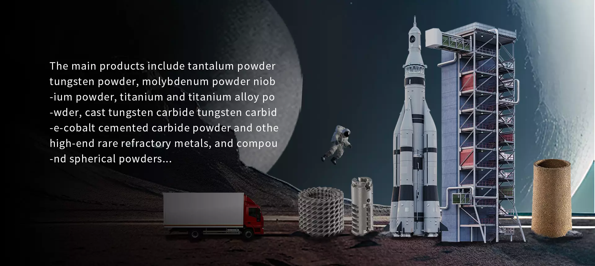
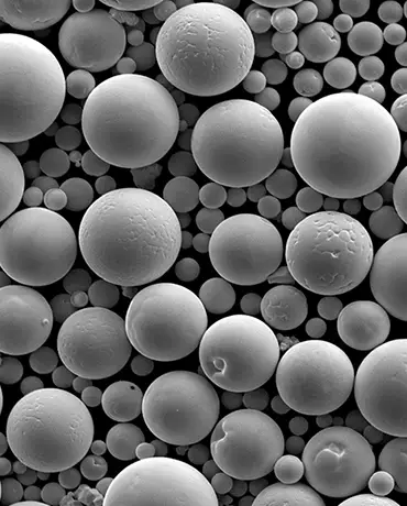
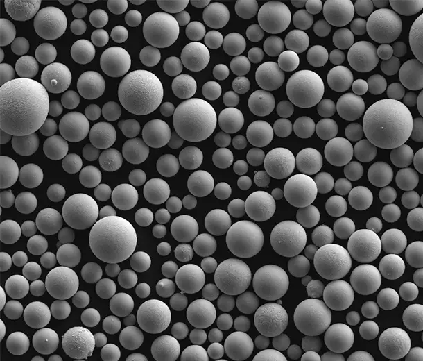
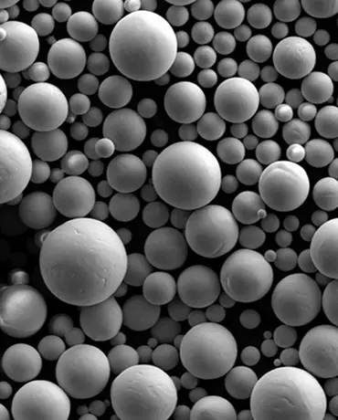
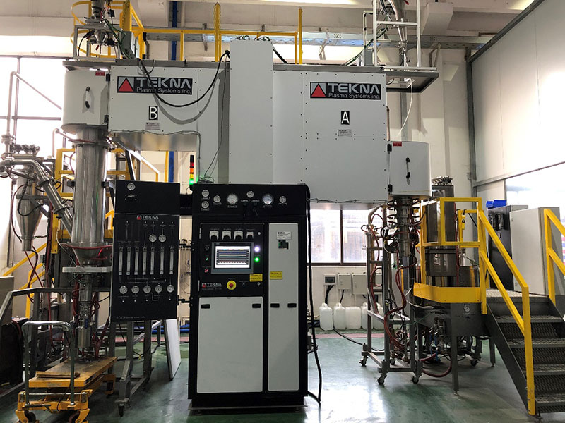
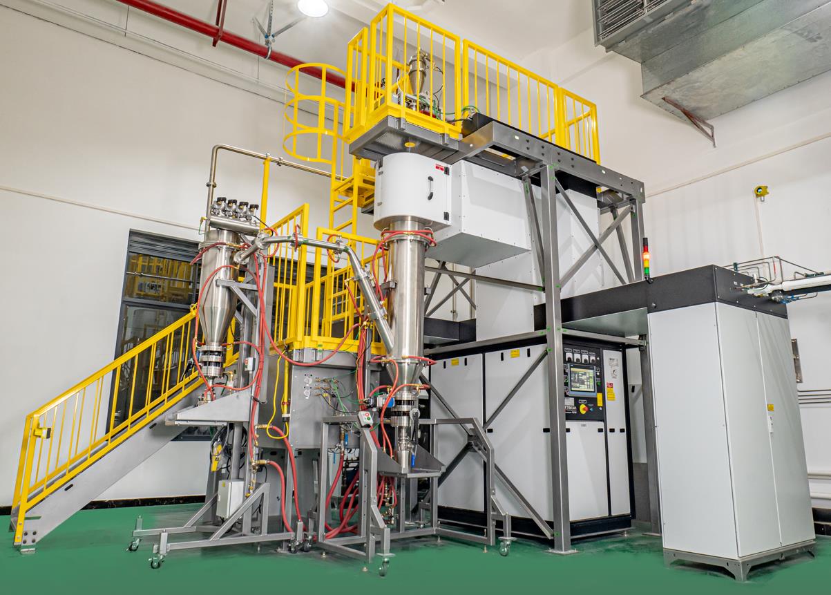
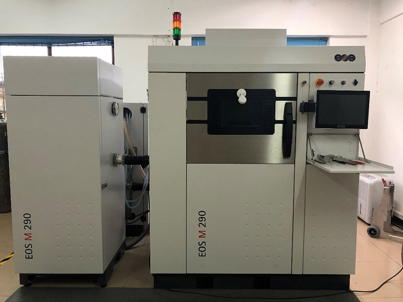
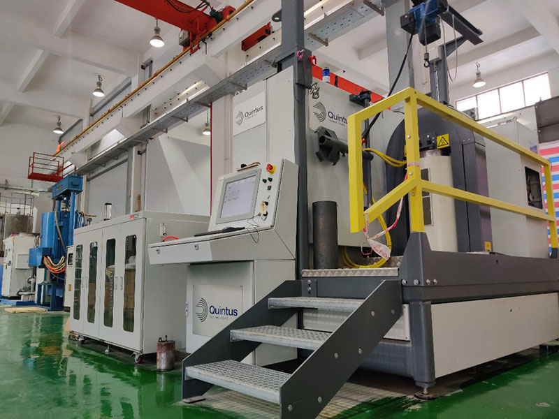
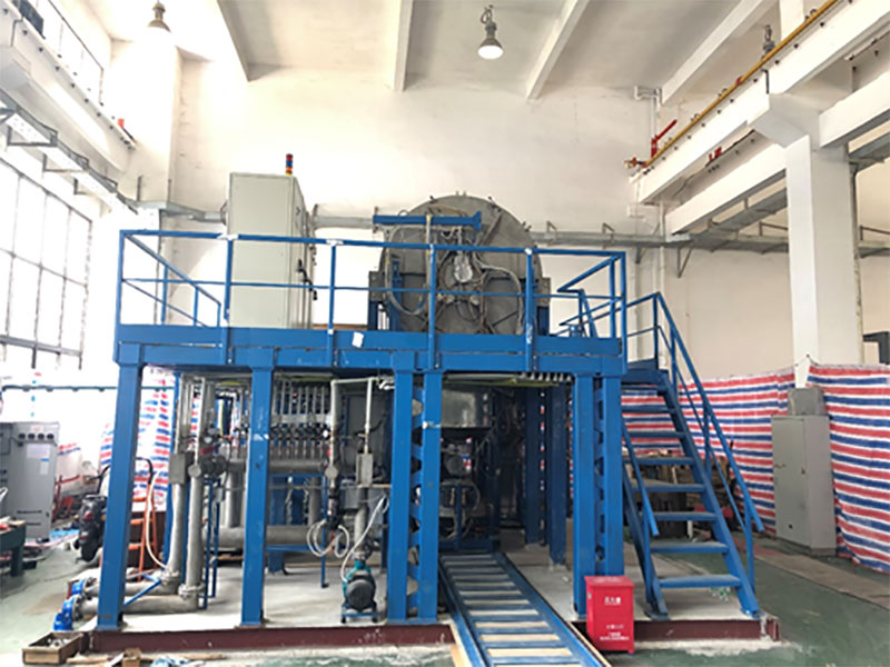
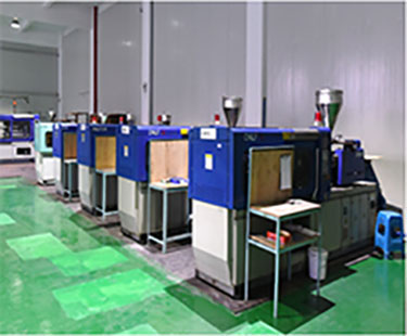
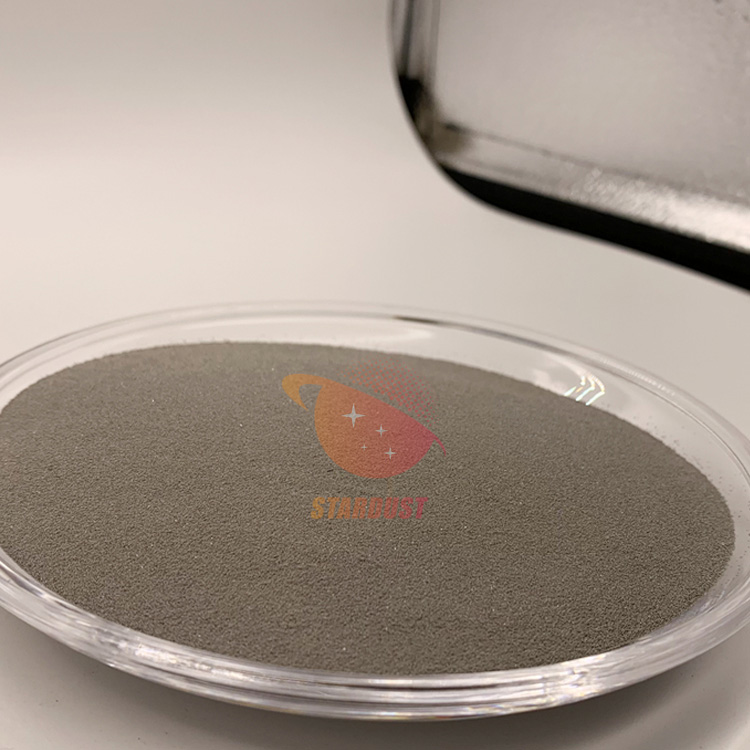
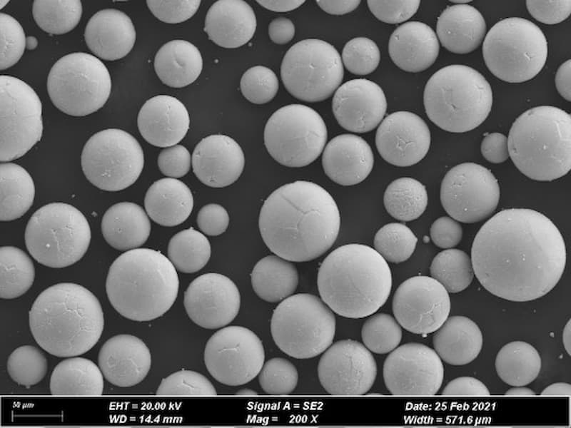
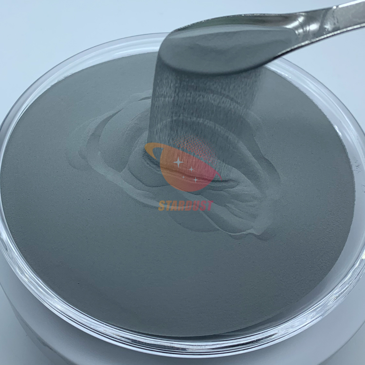
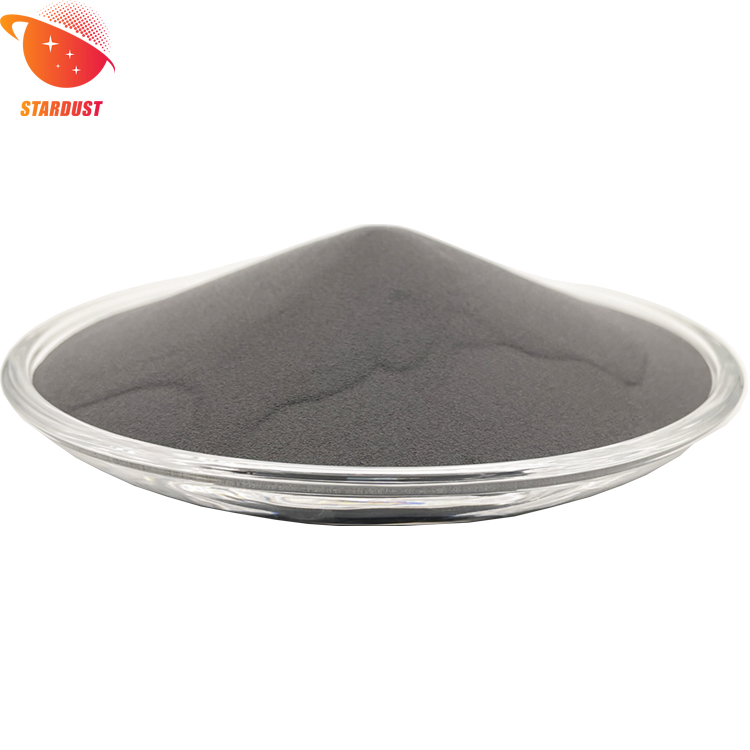
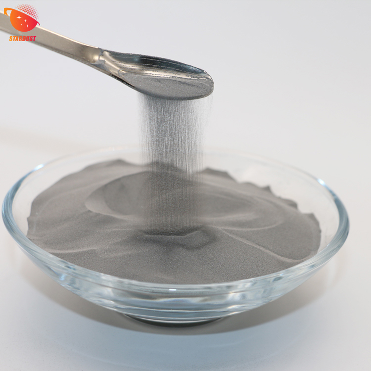
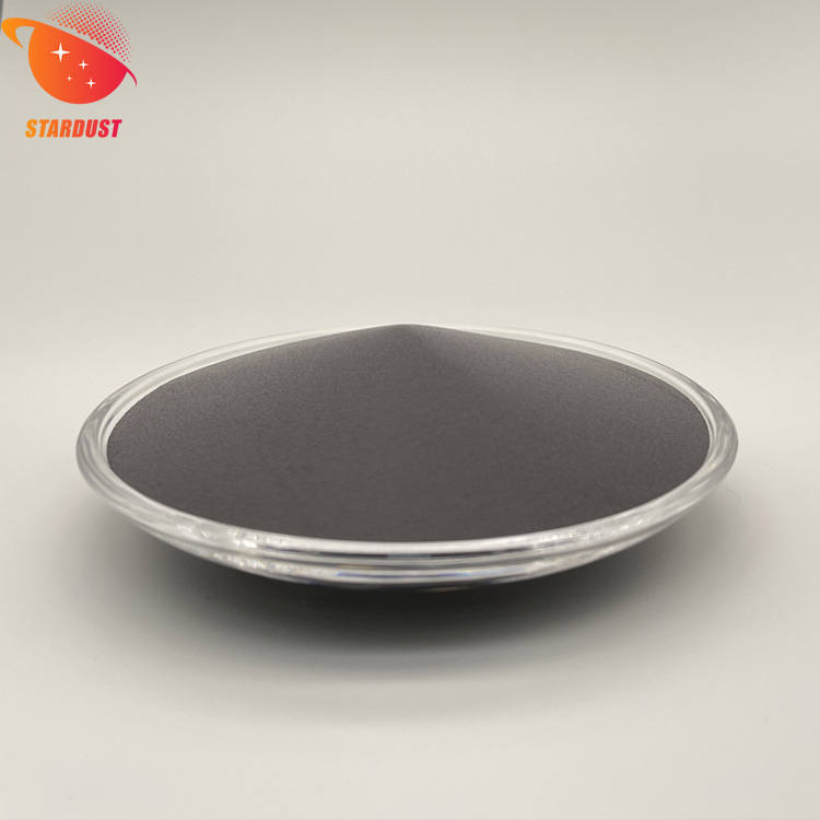
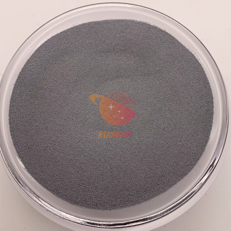
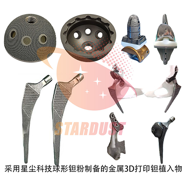
banner
News
Home

News

Analysis of microstructure and properties of Nb521 alloy formed by electron beam selective zone melting
New Products

Analysis of microstructure and properties of Nb521 alloy formed by electron beam selective zone melting

Oct 10, 2024

Nb521 alloy is a new type of niobium-tungsten alloy, the nominal composition of Nb-5W-2Mo-1Zr, with a high melting point (2630 ℃), moderate density 8.9g/cm3), high-temperature strength (1600 ℃, Rm ≥ 100MPa), machining and welding performance and other advantages [1,2], is expected to replace C103 (Nb-10Hf-1Ti) alloy to become a new generation of high temperature structural materials widely used in aerospace, nuclear and other industries [3]. Aerospace, nuclear industry and other industries widely used in the new generation of high-temperature structural materials [3]. The alloy is solid solution strengthened with Mo and W elements to improve the high temperature and room temperature strength of the alloy, and the active element Zr is added to improve the oxidation and corrosion resistance of the alloy.Zr can also be generated with the interstitial elements of carbon and oxygen to produce carbides and oxides, and play a role in purifying the grain boundaries or precipitation strengthening [4].

Electron beam selective melting forming technology (selectiveelectronbeammelting, referred to as SEBM) as a new metal additive manufacturing technology, with high energy utilization, high forming efficiency, low forming stress, vacuum clean and other advantages, solves the solution to take into account the complex shape and high performance of the metal components of the rapid manufacturing of the technical problems in the ‘High’, “fine”, “sharp” rare refractory metal complex precision components of the rapid development, structural and functional integration, etc. have shown unique advantages [5-7]. -7]. At present, electron beam selective melting forming technology has been widely used in titanium and titanium alloys [8, 9], stainless steel [10], tungsten [11], tantalum [12], TiAl intermetallic compounds [13, 14] and other brittle, refractory, high-activity metal materials, but in the forming of niobium and niobium alloys, the relevant reports are still relatively small. The authors also demonstrated the feasibility of SEBM for the preparation of superconducting RF cavity parts. In this study, we explored the SEBM forming process of Nb521 alloy, characterized the densification process, and made a detailed analysis of the microstructure and microhardness distribution characteristics of the prepared Nb521 alloy samples, and initially grasped the properties of niobium-tungsten alloy prepared by using E-beam Additive Manufacturing technology, which will open up a new way to broaden the application of Nb521 alloy for complex precision parts.

1  Experiment

1.1  Experimental materials

The experimental material is Nb521 powder produced by Xi'an Sailon Metal Materials Limited Liability Company (hereinafter referred to as Sailon), and its morphology is shown in Figure 1. The powder has a smooth surface, few satellite powders, >90% sphericity, >90% of the powder with a particle size between 53 and 150 μm, mobility of 12.1s/50g, bulk density of 5.2g/cm3, and vibration density of 5.75g/cm3.Table 1 shows the chemical composition of the Nb521 powder, and the impurity elements C, N, O, and H in the powder are low, and the O content is 0.022%.

Figure 1: Morphology of Nb521 powder prepared by plasma rotating electrode atomisation method.


1.2  Experimental process

The S2 type powder bed electron beam 3D printing equipment independently developed by Sailon was used to form the samples. The equipment mainly consists of electrical control cabinet, electron gun and power supply, vacuum forming chamber, feeding and laying powder mechanism, vacuum system, etc. The maximum forming size is 200mm×200mm, the maximum melting current is 50mA, the maximum hopping speed is 8000m/s, the accelerating voltage is 60kV, the diameter of the electron beam spot is ≤200μm, and the precision of part forming is ±0.3mm.The principle of the equipment printing is shown in Fig. 2.

Figure 2 schematic diagram of the principle of electron beam selective melting and forming

E-beam selective melt forming process: ① using modeling software to draw the print sample model, sample size of 12mm × 12mm × 10mm, stretching sample size of 12mm × 70mm × 12mm; ② the use of Sailon's self-developed SLEBMBuildPrepare software for the slicing and path planning, the layer thickness is set to 0.05mm, the melting pitch is set to 0.1mm, the two-dimensional melt forming process is obtained. 0.1mm, to obtain two-dimensional cross-section data and path planning data; ③ simulation data into the printer, set process parameters; ④ the use of e-beam scanning preheating base plate (700 ~ 900 ℃); ⑤ forming process in order to maintain the working temperature of the base plate, to ensure the stability of the printing process of the powder bed, preheating of the spread of the powder; ⑥ print a layer of the height of the base plate down a layer of the powder picker for the spread of the powder, the powder. Electron beam and then preheat, selective melting, until the entire part is printed. In order to reduce the directional difference in the performance of the printed part and reduce the unevenness of the temperature field distribution in the forming process, the scanning paths of the two adjacent levels are rotated by 90°. During the printing process, the temperature of the base plate rises slightly in the early stage and eventually stabilises, and the temperature change curve of the base plate during preheating and printing is shown in Figure 3.

1.3  Characterisation of properties

Formed Nb521 alloy samples were ground and polished, corroded with HCl+HNO3+HF mixed acid solution (2:2:1 by volume), and the transverse and longitudinal microstructures of the specimens were observed by metallographic microscopy. The chemical composition of the formed samples was determined using chemical analysis. The density of the samples was measured by drainage method. The physical structure of the samples was analysed by X-ray diffractometer. The room temperature tensile properties of the formed samples were determined by Instron-5982 universal testing machine. After removing the loose layer (about 0.7mm) from the exterior of the formed sample, and the surface was sanded and polished, a microhardness tester was used to measure the microhardness of the sample along the direction of the stacking height and at the stacking level, with a spacing of 1mm between the test points, a load of 1.96N, and a loading time of 15 s. Fig. 4 shows the schematic diagram of microhardness measurement points.

Fig. 3 Temperature change curve of the base plate in the process of electron beam selective melting and forming

Figure 4 Schematic diagram of microhardness test points

2  Results and Discussion

2.1  Effect of melting process on densification

The electron beam energy received by the powder is measured in terms of line energy density and calculated as shown in equation (1).

E=IU/(vht)(1) where:I is the melting current; U is the accelerating voltage, 60kV; v is the melting speed; h is the melting spacing; t is the layer thickness of the laid powder. In this study, the layer thickness and the melting spacing are kept constant, and the forming quality of Nb521 alloy is mainly determined by the two parameters of melting current and melting speed. Figure 5 shows the macroscopic photographs of Nb521 alloy samples and the morphology of internal defects under different electron beam energy densities. From Fig. 5, it can be seen that with the increase of the electron beam energy density, the melting quality of the printed samples ranges from undermelt to good and then to overmelt state. Due to the limited depth of the melt pool in the under-melting state, there is poor interlayer bonding, resulting in more seam defects distributed along the layers; in the over-melting state, the energy input is too high, which is prone to local overheating, and the stability of the melt pool is poor, which is prone to produce defects such as shrinkage holes. When the energy density of the melt pool is 340J/mm3, it has the best fusion quality, and no defects such as cracks and poor fusion are seen within the field of view.

Fig. 5 Macroscopic photographs of Nb521 alloy samples with different electron beam energy densities and the morphology of internal defects

Combined with the above forming quality analysis, the forming process window of Nb521 alloy was formed as shown in Fig. 6. The fusion quality is better when the melting speed is 0.3-0.35 m/s and the melting current is 8-9 mA; the fusion quality is poor when the melting current is 10-13 mA and the speed is 1.0-2.0 m/s; and the phenomena of over-melting and deformation warping appear when the melting current is 12-13 mA and the speed is 0.3 m/s. The density of the formed samples under the optimal process was measured as 8.78-8.79g/cm3 using the drainage method, which meets the density requirements of niobium-tungsten alloy rods for aerospace use (8.65-9.00g/cm3) [16].

Fig. 6 SEBM forming Nb521 alloy process window


2.2  Chemical composition

Table 2 shows the chemical composition of the Nb521 alloy samples. Compared with the chemical composition of Nb521 powder in Table 1, the content of W, Mo, Zr alloying elements in the formed parts has no significant change compared with the powder. Due to the clean environment of electron beam forming, the C and N contents in the formed samples were significantly reduced, the H content did not change significantly, and the oxygen content increased by only 0.005%.

2.3  Microstructure

Figure 7 shows the microstructure of the longitudinal cross-section (i.e. along the deposition direction) of the SEBM-formed Nb521 alloy samples.The grains of the SEBM-formed samples are columnar crystals growing from the bottom, and the columnar crystals run through the entire direction of the deposition height, and the widths of the columnar crystals vary from 5 to 100 μm. The layer band structure between layers is obvious in Fig. 7, which is the interface between the molten pool and the solidified layer, and is a trace of the formation of channels/layers.

Figure 7 Microstructure of longitudinal section of Nb521 alloy sample

Figure 8a shows the microstructure of the deposition level of the formed sample perpendicular to the deposition direction. In addition to the visible large-size columnar crystals in Fig. 8a, a small number of equiaxed crystals are unevenly distributed, with grain sizes ranging from 20 to 100 μm. In response to this phenomenon, the microstructure analysis of the edge part of the formed sample block was carried out, and it was found that the same equiaxial crystal organisation was found near the edge part (Fig. 8b). This phenomenon may be related to the fast heat diffusion and large temperature gradient in the edge part, and there is no condition for the grains to continue to grow, while the equiaxed crystals existing inside the sample block may be related to the uneven distribution of the temperature field.

Figure 8 Microstructure of transverse section of Nb521 alloy sample

2.4  Physical phase composition

Figure 9 shows the XRD patterns of Nb521 powder and SEBM formed Nb521 alloy samples. From the XRD patterns of the powder, it can be seen that 38.6°, 55.7°, 69.9° and 82.8° correspond to the diffraction peaks of the crystal planes of the Nb matrix phase (110), (200), (211) and (220), respectively, and there are no other diffraction peaks, and the diffraction peaks of the Nb matrix phase are shifted to a high angle, which is related to the fact that the radii of the W and Mo atoms are smaller than that of Nb, and the solid dissolution into Nb leads to the lattice constant This is related to the fact that the lattice constant of W and Mo solid solution in Nb is smaller than that of Nb. In addition to the Nb matrix phase, a small amount of Nb2C and ZrC precipitated phases are also present in the XRD patterns of the formed samples. Compared with the diffraction peaks of Nb521 powder, the intensity of the formed sample is significantly enhanced at the (200) crystal plane, indicating a strong preferential growth orientation of the grains along the (200) crystal plane. This is consistent with the grain organisation and morphology in the metallographic observations. In addition, the diffraction peaks of the Nb matrix of the formed samples are shifted to a lower angle, which is closely related to the precipitation of some carbide phases leading to a larger lattice constant.

Figure 9 XRD patterns of Nb521 powder and Nb521 alloy samples


2.5  Tensile properties and hardness

The room temperature tensile stress-strain curves of SEBM formed Nb521 alloy samples are shown in Figure 10. The tensile strength of the formed sample reaches 384MPa, the yield strength is 307MPa, and the post-break elongation is 16.5%, which basically meets the mechanical property requirements in GJB8507-2015 Specification for Aerospace Niobium-Tungsten Alloy Bars, but there is still a small gap, mainly due to the following reasons: ① The density of formed Nb521 alloy meets the standard requirements, but the densification still needs to be improved, and the hardness of Nb521 alloy still needs to be improved, but the density of Nb521 alloy still needs to be improved. The main reasons include the following: ① forming Nb521 alloy density, although the standard requirements, but the density is still to be improved; ② from the sample of the layer and layer combination of the road traces, forming quality is still to be improved; ③ grains along the deposition direction of the columnar crystals, coarse size, the axial perpendicular to the direction of deposition of the tensile specimen, that is, the tensile stress is perpendicular to the columnar crystals, and columnar crystals between the grains of the occlusion is limited, the combination of high strength; ④ due to the electron beam selective melting and shaping is a rapid melting ④ Because the electron beam selective zone melting and forming is a rapid melting and cooling solidification process, the strengthened phase carbide is not enough time to fully precipitate, the precipitates are sub-stable phase, and the distribution is not uniform, so the strengthening effect is not obvious.

Fig. 10 Room temperature tensile stress-strain curves of Nb521 alloy samples

The microhardness distribution of Nb521 alloy samples along the stacking vertical direction (Z direction) and along the stacking level (XY plane) were tested respectively, and the results are shown in Fig. 11. It can be seen from Fig. 11 that the microhardness of the samples, both in the vertical direction and in the level, is in the range of 1500-1700 MPa. The measured microhardness of the samples did not fluctuate with the location of the measurement point, and the microhardness is isotropic.

Figure 11 Microhardness distribution of Nb521 alloy samples


3  Conclusion

(1) Using SEBM to form Nb521 alloy, when the density of the electron beam energy input is 340J/mm3, basically eliminates the fusion defects, and the density of the formed sample reaches 8.78-8.79g/cm3.

(2) SEBM forming Nb521 alloy microstructure along the deposition direction presents typical columnar crystal characteristics, due to the temperature field distribution and temperature gradient of the regional differences in the deposition level edge of the existence of a small number of equiaxial crystals.

(4) SEBM forming Nb521 alloy samples along the (200) crystal surface has a strong preferential growth orientation. In addition to the Nb matrix phase, a small amount of Nb2C and ZrC carbide precipitation phases are also present in the formed sample.

(5) The tensile strength of SEBM-formed Nb521 alloy reaches 384 MPa, the elongation after break is 16.5%, the microhardness is between 1500 and 1700 MPa, and there is no anisotropy along the deposition pendant and deposition level, and the mechanical properties basically meet the requirements for aerospace applications.

Reference: https://xueshu.baidu.com/usercenter/paper/show?paperid=1j6u0r70vh4204y0c82e0mv03e490089&site=xueshu_se

Stardust Technology (Stardust Technology) uses RF plasma spheroidisation technology to prepare spherical Nb521 alloy powders with the following characteristics and properties:

1. High sphericity: Through the RF plasma spheroidisation process, the Nb521 alloy powder can achieve extremely high sphericity, improving powder flow and packing density, which is very suitable for high-precision applications such as additive manufacturing (3D printing).

2. High purity: During the RF plasma spheroidisation process, the impurity content of the powder is greatly reduced, which ensures the high purity of Nb521 alloy, and thus improves the physical and chemical properties of the material.

3. Controllable particle size distribution: Through fine adjustment of process parameters, Stardust is able to produce spherical Nb521 alloy powders with different particle size distributions to meet the needs of different industrial applications.

4. Excellent mechanical properties: After metallurgy and processing, the spherical Nb521 alloy powder shows excellent strength, toughness and creep resistance, which is especially suitable for the manufacture of key components in aerospace and high temperature fields.

The high sphericity and excellent properties of the powder make it a widely used prospect in the fields of additive manufacturing and powder metallurgy.

Welcome to contact our manager Cathie Zheng +86 1331 8326 187

Need Help? leave a message

leave a message
If you are interested in our products and want to know more details,please leave a message here,we will reply you as soon as we can.
Send

Home

products

whatsApp

contact